
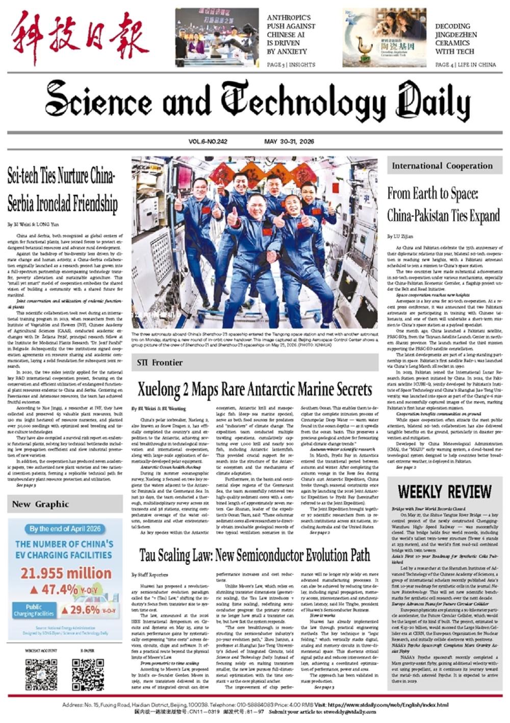
 Next
Next


Huawei has proposed a revolutionary semiconductor evolution paradigm called the "τ (Tau) Law," shifting the industry's focus from transistor size to system time cost.
The law, announced at the 2026 IEEE International Symposium on Circuits and Systems on May 25, aims to sustain performance gains by systematically compressing "time costs" across devices, circuits, chips and software. It offers a practical route beyond the physical limits of Moore's Law.
From geometric to time scaling
According to Moore's Law, proposed by Intel's co-founder Gordon Moore in 1965, more transistors delivered in the same area of integrated circuit can drive performance increases and cost reductions.
Unlike Moore's Law, which relies on shrinking transistor dimensions (geometric scaling), the Tau Law introduces τ scaling (time scaling), redefining semiconductor progress: the primary metric is no longer how small a transistor can be, but how fast the system responds.
"The core breakthrough is reconstructing the semiconductor industry's 50-year evolution path," Zhou Jianjun, a professor at Shanghai Jiao Tong University's School of Integrated Circuits, told Science and Technology Daily. Instead of focusing solely on making transistors smaller, the new law pursues full-dimensional optimization with the time constant τ as the core physical anchor.
The improvement of chip performance will no longer rely solely on more advanced manufacturing processes. It can also be achieved by reducing time delay, including signal propagation, memory access, interconnection and synchronization latency, said He Tingbo, president of Huawei's Semiconductor Business.
How it works
Huawei has already implemented the law through practical engineering methods. The key technique is "logic folding," which vertically stacks digital, analog and memory circuits in three-dimensional space. This shortens critical signal paths and reduces interconnect delays, achieving a coordinated optimization of performance, power and area.
The approach has been validated in mass production.
Huawei has designed and manufactured 381 chips over the past six years based on this framework.
The Kirin 2026 chip, to be launched in autumn, will be the first full implementation of logic folding, expanding from single-layer to dual-layer design. By 2031, Huawei expects its high-end chips to achieve transistor density equivalent to the 1.4nm process node.
Industry impact
The Tau Law is expected to reshape the semiconductor industry's basic development principles.
First, it shifts the focus of semiconductor evolution from geometric scaling to time scaling, and based on this framework, progress will depend on full-stack collaboration covering devices, architectures, software and systems, rather than on lithography scaling alone.
Second, it provides strategic guidance for supply chains. "Chip manufacturing does not need to rely excessively on cutting-edge lithography equipment," Zhou said. Advanced packaging will gain strategic importance, and circuit innovation, architectural changes, and system-level optimization can help close the process technology gap to deliver high-performance chips.
However, since it is a newly proposed methodology, the Tau Law's applicability across different scenarios and its full adaptation to existing electronic design automation tools and ecosystems still require further validation and optimization.